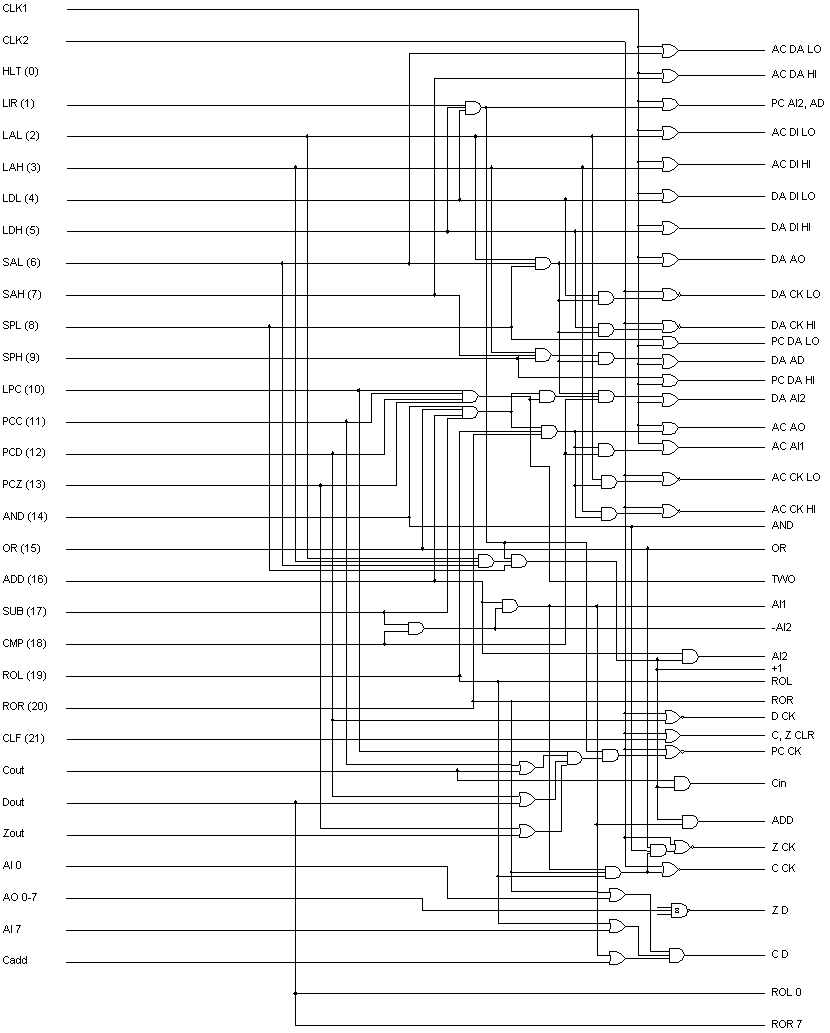
Due to the complexity of the Arithmetic Logic Unit, and the way it interacts with the processor's internal registers (accumulator, data address register, and program counter) I developed a wiring diagram that shows how the components of these are interconnected. Signal names on the left are those of the decoded microcode instructions, clock signals, and data/flag lines. Signal names on the right are those of various signals internal to the ALU and registers; the names should be self-explanatory. (E.g., DA AO is the name of the signal that enables, in the data address register, the 74LS244 that places the contents of this register on the address bus.) I also used these symbols when I labelled the chips (seen on the processor's photograph), to make the assembly process less error-prone.
The top half of the completed computer, as seen in the picture, contains the TTL logic chips that implement the above diagram, chips that comprise the Arithmetic Logic Unit, plus chips that make up the processor's accumulator, program counter, and data address register.
The bottom half of the computer contains the microcode ROM and microcode decoder, RAM, switches used to program the ROM and RAM, and the CPU clock. A 40-pin connector is used to connect the two halves via a short piece of ribbon cable.